Graphene: The Atomic Marvel Reshaping Our Technological Landscape
In the realm of materials science, few discoveries have sparked as much excitement and promise as graphene. This two-dimensional wonder material, composed of a single layer of carbon atoms arranged in a hexagonal lattice, has captured the imagination of scientists, engineers, and innovators worldwide. As we delve into the atomic structure and composition of graphene, we'll uncover the secrets behind its extraordinary properties and explore its potential to revolutionize industries ranging from electronics to energy storage.
The Atomic Architecture of Graphene
At its core, graphene is deceptively simple. It consists entirely of carbon atoms, the same element found in pencil lead and diamonds. However, it's the unique arrangement of these atoms that sets graphene apart. Imagine a sheet of paper, but millions of times thinner – that's the scale we're dealing with when we talk about graphene.
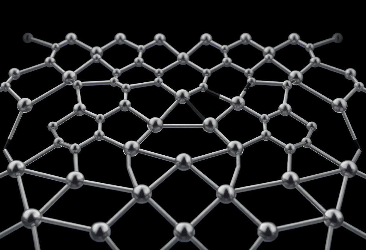
Each carbon atom in graphene is bonded to three neighboring carbon atoms, forming a repeating pattern of hexagons that resembles a honeycomb or chicken wire. This structure is just one atom thick, making graphene the world's first two-dimensional material. Despite its incredible thinness, graphene sheets can span surprisingly large areas, with some laboratory-produced samples reaching sizes of up to 30 inches.
The carbon atoms in graphene are held together by strong covalent bonds known as sigma (σ) bonds. These bonds give graphene its remarkable strength – about 200 times stronger than steel by weight. But what truly sets graphene apart is the presence of a fourth electron from each carbon atom that isn't used in these sigma bonds. Instead, these electrons form weaker pi (π) bonds that are delocalized across the entire graphene sheet. This delocalization is key to understanding many of graphene's unique electronic properties.
The Quantum Realm of Graphene
When we zoom in to the quantum level, graphene reveals even more fascinating characteristics. The electrons in graphene behave in ways that defy classical physics, moving as if they have no mass and traveling at speeds approaching that of light. This behavior is more akin to particles described by quantum electrodynamics than traditional electrons in metals or semiconductors.
One of the most intriguing quantum phenomena exhibited by graphene is the anomalous quantum Hall effect. Usually observed only at extremely low temperatures in other materials, this effect can be seen in graphene even at room temperature. This property, along with graphene's high electron mobility, makes it a promising candidate for quantum computing applications.
The unique band structure of graphene also leads to the phenomenon of Klein tunneling, where electrons can pass through potential barriers with perfect transmission. This effect, predicted by quantum mechanics but difficult to observe in most materials, is readily apparent in graphene, offering new avenues for studying fundamental physics and developing novel electronic devices.
Beyond Pure Graphene: Modifications and Variants
While pristine graphene is remarkable on its own, scientists have found ways to modify and enhance its properties through various techniques. One approach is functionalization, where other molecules or atoms are attached to the graphene sheet. This can alter graphene's chemical reactivity, solubility, and electronic properties, tailoring it for specific applications.
Doping, the process of introducing impurities into the graphene lattice, is another powerful tool for modifying its properties. By carefully controlling the type and concentration of dopants, researchers can fine-tune graphene's electronic characteristics, potentially enabling new types of electronic and optoelectronic devices.
Graphene oxide, a form of graphene with oxygen-containing groups attached to its surface, has gained significant attention in recent years. While it lacks some of graphene's exceptional electronic properties, graphene oxide is easier to produce in large quantities and can be chemically reduced to form a graphene-like material. This has opened up new avenues for large-scale production and application of graphene-based materials.
Three-Dimensional Graphene Structures
Although graphene is fundamentally a two-dimensional material, researchers have developed various ways to create three-dimensional structures from graphene sheets. These 3D forms often combine the unique properties of 2D graphene with new characteristics that emerge from their three-dimensional architecture.
Graphene aerogels, for instance, are ultra-light, sponge-like structures made from interconnected graphene sheets. These materials can have densities as low as 0.16 mg/cm³, making them among the lightest solid materials known. Despite their low density, graphene aerogels maintain exceptional electrical conductivity and high surface area, making them promising for applications in energy storage, catalysis, and environmental remediation.
Another interesting 3D form is few-layer graphene, consisting of stacks of 2-10 graphene layers. These structures can exhibit properties intermediate between those of single-layer graphene and bulk graphite, offering new possibilities for tailoring material characteristics.
Production Methods and Their Impact on Graphene Quality
The method used to produce graphene can significantly affect its structure, quality, and properties. The famous "scotch tape" method, also known as mechanical exfoliation, was used to isolate graphene for the first time. While this method produces high-quality graphene flakes, it's not suitable for large-scale production.
Chemical vapor deposition (CVD) has emerged as one of the most promising methods for producing large-area graphene sheets. In this process, a carbon-containing gas is exposed to a metal substrate at high temperatures, causing carbon atoms to deposit and form a graphene layer. CVD can produce graphene sheets up to several square meters in size, although the quality is generally lower than that of mechanically exfoliated graphene.
Epitaxial growth on silicon carbide is another method that can produce high-quality graphene directly on a semiconductor substrate. This technique is particularly promising for electronic applications, as it eliminates the need to transfer graphene from a metal substrate to a semiconductor.
The Broader Family of 2D Materials
The discovery of graphene has led to a surge of interest in other two-dimensional materials. Hexagonal boron nitride (h-BN), often called "white graphene," has a similar structure to graphene but consists of alternating boron and nitrogen atoms. It's an excellent insulator and can be used as a substrate for graphene devices.
Transition metal dichalcogenides (TMDs), such as molybdenum disulfide (MoS2) and tungsten diselenide (WSe2), form another important class of 2D materials. These materials can be semiconducting or metallic and offer a range of optical and electronic properties not found in graphene.
Phosphorene, a 2D form of phosphorus, has also garnered significant attention. It has a unique puckered structure that gives it highly anisotropic electronic and thermal properties, making it interesting for thermoelectric applications and field-effect transistors.
Challenges and Future Prospects
Despite its immense potential, graphene faces several challenges on its path to widespread adoption. Producing high-quality, large-area graphene at a reasonable cost remains a significant hurdle. Additionally, integrating graphene into existing manufacturing processes and technologies presents its own set of challenges.
The lack of a bandgap in pristine graphene limits its use in certain electronic applications, particularly in digital logic circuits. While various methods have been developed to induce a bandgap in graphene, such as creating nanoribbons or applying strain, each comes with its own trade-offs in terms of performance and manufacturability.
Nevertheless, the future of graphene looks bright. Research into graphene and other 2D materials continues at a rapid pace, with new discoveries and potential applications emerging regularly. From next-generation electronics and energy storage devices to advanced sensors and biomedical applications, graphene has the potential to touch nearly every aspect of our technological lives.
As we continue to unlock the secrets of this atomic marvel, we're not just exploring a new material – we're potentially laying the groundwork for the next technological revolution. The story of graphene serves as a powerful reminder of how fundamental scientific research can lead to transformative technologies, and it underscores the importance of continued investment in basic science and materials research.
In conclusion, graphene's journey from a theoretical curiosity to a material at the forefront of technological innovation is a testament to the power of scientific inquiry and human ingenuity. As we stand on the brink of a new era in materials science, graphene lights the way forward, promising a future where the boundaries between the possible and impossible continue to blur.